Technology
Samsung Invests $773 Million in ASML to Boost Chip Manufacturing
Samsung Electronics Co., a prominent player in the memory chip sector, has made a significant investment in semiconductor technology. The South Korean company is set to acquire two advanced extreme ultraviolet (EUV) lithography machines from ASML Holding N.V. for approximately 1.1 trillion won (about $773 million). This strategic move aims to enhance Samsung’s capabilities in next-generation semiconductor manufacturing and regain its competitive edge in the global chip market.
According to industry sources, Samsung anticipates receiving its first high-numerical-aperture (high NA) EUV scanner, known as the Twinscan EXE:5200B, by the end of this year. The second unit is expected to be delivered in the first half of 2026. While Samsung currently operates a research-use high NA EUV tool at its Hwaseong campus, these new machines will be the company’s first dedicated to mass production.
The high NA EUV technology, developed exclusively by ASML, significantly improves manufacturing efficiency. It can etch circuits with a precision that is 1.7 times finer than circuits produced with current-generation EUV tools. This enhancement stems from an increase in the system’s numerical aperture, which has risen from 0.33 to 0.55. Each unit carries a hefty price tag of around 550 billion won, making them the most costly equipment in semiconductor manufacturing.
Samsung’s Chairman, Jay Y. Lee, has shown a keen interest in high NA EUV technology since visiting ASML’s headquarters in December 2023. Impressed by the potential of this technology to produce chips below the 2-nanometer threshold, Lee has reportedly directed engineers to expedite the development of compatible processes. The decision to incorporate these advanced tools into production indicates that Samsung’s engineering teams have reached a critical stage in their technology roadmap.
While Samsung is moving forward with these purchases, competitors like TSMC and Intel Corp. are still testing research and development versions of the high NA EUV systems without committing to commercial-scale manufacturing. Notably, SK Hynix is the only other company known to have secured a production-grade high NA EUV unit, which was announced in September.
Strategic Move for AI-Driven Semiconductor Production
Samsung has a history of innovation in semiconductor technology, having been the first to implement conventional EUV lithography in its 7 nm foundry line in 2018 and subsequently in DRAM production in 2020. The introduction of high NA EUV systems marks a significant leap forward, enabling ultra-precise patterning essential for advanced chips that support artificial intelligence and data-intensive applications.
The new machines will be deployed at Samsung’s 2 nm foundry lines, which already manufacture the Exynos 2600 application processors. Additionally, the company plans to produce next-generation AI chips for Tesla Inc. using this cutting-edge EUV technology. These machines will also facilitate the production of Samsung’s future vertical channel transistor (VCT) DRAM, a high-performance memory chip slated for mass production around 2027.
Analysts view this investment as a clear signal that Samsung is shifting back into an aggressive investment mode. After a period of cautious capital spending, the company is taking decisive steps to narrow the performance gap with competitors, particularly TSMC, the leading player in the foundry sector. Recently, Samsung has also made strides in high-bandwidth memory (HBM) technology, announcing plans to enhance data rates for its upcoming HBM4E chips to 13 gigabits per second per pin, surpassing current industry offerings.
As the semiconductor landscape evolves, Samsung’s early adoption of high NA EUV technology may serve as a pivotal factor in re-establishing its leadership in both logic and memory sectors, especially as demand for AI computing continues to reshape the industry.

Financial Markets Indicate Commodities ‘Supercycle’ by 2026
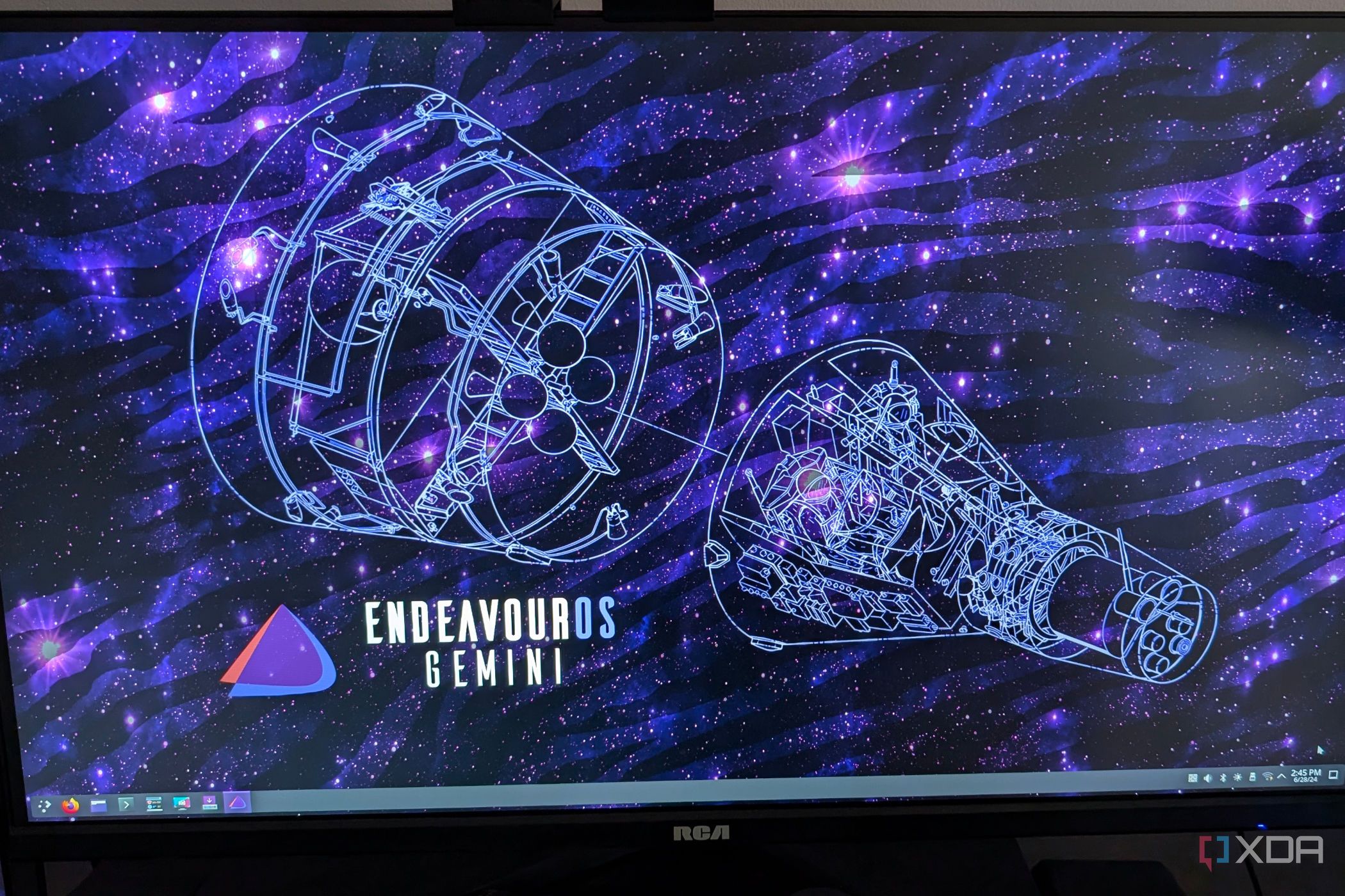
EndeavourOS Simplifies Arch Experience Without Installation Hassles
Bears Shock Packers with Historic Wild Card Comeback Victory
NBA Sunday Showdown: Injuries and Returns Impact Fantasy Picks

Local Students Celebrate Graduation from Penn State Berks and More
Rachel Campos-Duffy Exits FOX Noticias; Andrea Linares Steps In
Piper Rockelle Shatters Record with $2.3M First Day on OnlyFans

Meta’s 2026 AI Policy Sparks Outrage Over Privacy Concerns
Leon Goretzka Considers Barcelona Move as Transfer Window Approaches
Urgent Update: Denver Fire Forces Mass Evacuations, 100+ Firefighters Battling Blaze
-
 Top Stories1 month ago
Rachel Campos-Duffy Exits FOX Noticias; Andrea Linares Steps In
-
 Top Stories1 week ago
Piper Rockelle Shatters Record with $2.3M First Day on OnlyFans
-
Top Stories6 days ago
Meta’s 2026 AI Policy Sparks Outrage Over Privacy Concerns
-
 Sports5 days ago
Leon Goretzka Considers Barcelona Move as Transfer Window Approaches
-
 Top Stories1 week ago
Urgent Update: Denver Fire Forces Mass Evacuations, 100+ Firefighters Battling Blaze
-
 Top Stories1 week ago
OnlyFans Creator Lily Phillips Reconnects with Faith in Rebaptism
-
 Entertainment5 days ago
Tom Brady Signals Disinterest in Alix Earle Over Privacy Concerns
-
 Top Stories7 days ago
Oregon Pilot and Three Niece Die in Arizona Helicopter Crash
-
 Top Stories5 days ago
Warnock Joins Buddhist Monks on Urgent 2,300-Mile Peace Walk
-
 Health2 months ago
Terry Bradshaw Updates Fans on Health After Absence from FOX NFL Sunday
-
 Top Stories4 days ago
CBS Officially Renames Yellowstone Spin-off to Marshals
-
 Sports3 days ago
South Carolina Faces Arkansas in Key Women’s Basketball Clash